

The FTL (Flash Translation Layer) is the part of the firmware embedded in a storage device's controller that sits between the operating system and the physical NAND memory. It is the "brain" that makes an inherently complex and limited technology behave like a traditional storage device. It is present in SSDs, USB sticks and SD and microSD cards: every device built on NAND flash technology.
Why does the FTL exist?
NAND flash memory has fundamental limitations:
- Data cannot be overwritten in place: whole blocks must be erased first.
- Cells wear out: every write and erase cycle degrades them.
- Blocks fail: defective blocks have to be detected and mapped out.
- Writes are slow compared with reads.
- Reading degrades too: every read operation electrically disturbs the neighbouring cells (see point 7).
The FTL hides all this complexity from the operating system, presenting a simple interface of logical blocks that appears to work like a traditional storage device.
Main functions of the FTL
1. Translating logical addresses into physical ones
When the operating system asks to write to "block 1000", the FTL:
- Looks up its mapping table (held in RAM and in the NAND itself).
- Finds a free physical location, which may be on any chip.
- Writes the data there.
- Updates the table so that "logical block 1000" points to that physical location.
Key point: the same logical address can point to a different physical location after every write.
2. Wear levelling
The problem: if data were always written to the same physical blocks, those would wear out quickly while the rest stayed untouched. The FTL's solution:
- Dynamic wear levelling: rotates the physical locations of data that changes often.
- Static wear levelling: occasionally moves "cold" data (data that does not change) onto heavily used blocks, and vice versa.
- Result: wear is spread evenly across all cells, maximising service life.
3. Garbage collection
The problem: writes happen at page level (4 to 16 KB), but erases happen at block level (several MB). How it works:
- When data is updated, the FTL writes the new version to a free location and marks the old one as invalid.
- Over time, blocks become fragmented, mixing valid and invalid pages.
- The collector consolidates the valid pages from several blocks into a single one.
- It then erases the blocks that are left empty, freeing space.
This happens in the background, but it can affect performance when the device is very full.
4. ECC (error-correcting code)
NAND memory is prone to bit errors. Under the FTL's management, the controller implements:
- BCH (Bose-Chaudhuri-Hocquenghem): simpler codes, used in older devices.
- LDPC (Low-Density Parity-Check): more powerful codes, used in modern NAND flash chips, able to correct more errors.
Process:
- On write: it calculates the check codes and stores them alongside the data.
- On read: it verifies integrity and corrects errors automatically.
- If the errors exceed its correction capacity, it marks the block as defective.
5. Encryption
Many devices implement hardware encryption (AES-256), managed by the controller transparently to the user:
- It encrypts data before writing it to the NAND.
- It decrypts it when reading.
- The key may be password-based (as with BitLocker) or transparent.
- Effect on secure erase: deleting the encryption key is enough to make all the data unrecoverable instantly.
6. Real-time compression
Some controllers compress data before writing it:
- Advantage: better performance and endurance, because fewer physical writes are needed.
- Disadvantage: inconsistent performance, depending on how compressible the data is.
7. Read disturb
The problem: NAND cells do not only degrade when they are written. Every read operation induces an electrical disturbance in the neighbouring cells of the same block, and that disturbance accumulates with the number of reads.
Physical mechanism: to read a cell, the controller has to apply a high pass voltage —in the order of 6 volts— to all the other cells sharing the same connection line. That voltage does not reach the programming voltage, which is around 15 volts, but it has a weak programming effect on the cells it is applied to. In other words: reading applies voltage, and voltage programs a little.
Consequence: an area of memory can become unreadable without ever having been written to, simply because it has been read many times.
Where it shows up first: in the FTL's own mapping tables. The controller has to consult them on every access to the device, so they accumulate far more reads than any stored file. A file may go months without being opened; the table that says where that file is gets read hundreds of times a day.
The FTL's solution: the controller keeps read counters per block and, once a given threshold is passed, rewrites the data elsewhere to restore the charge levels. This mechanism has limits, and how well it works depends on the memory technology and on how worn the block is.
Relationship with density: the effect grows both with the number of reads and with the write and erase cycles the block has accumulated. It is most severe on cells with a lower threshold voltage, because the impact correlates with the difference between the pass voltage and the cell's own voltage. In SLC, with two levels, the margin is wide and the accumulation is irrelevant. In QLC, with sixteen levels squeezed into the same electrical range, a disturbance that would have no effect at all on SLC can be enough to make the data unreadable.
Practical consequence for data recovery
When a device shows this kind of deterioration, every additional read attempt on the affected area makes it worse. That is why the laboratory stops all uncontrolled access to the device and works with specialist instruments instead of the operating system.
This phenomenon has been characterised experimentally in peer-reviewed scientific literature. The references are listed at the end of the article.
Why is it so complex?
The FTL is an extraordinarily complex piece of engineering that turns a hard-to-govern technology into something that works transparently. Its design is one of each manufacturer's best-kept secrets, and the difference between a good FTL and a bad one can be the difference between an excellent SSD and a mediocre one.
Scrambling
NAND memory works best with random data patterns. So the controller:
- Runs the data through a randomisation algorithm before writing it.
- Turns uniform sequences such as "00000000" into pseudo-random patterns.
- Reason: it improves cell reliability and the effectiveness of the ECC.
Interleaving
In devices with several NAND chips connected over several channels, the FTL:
- Spreads a large write across several chips and channels in parallel.
- Example: a 1 MB write can be split into eight 128 KB fragments, each sent to a different chip at the same time.
- Result: a performance multiplier. A device with eight channels can be up to eight times faster.
Complex address mapping
The FTL does not keep a simple one-to-one mapping. It uses sophisticated structures:
- Page-level mapping: a large table linking each logical page to its physical location. It requires plenty of RAM.
- Hybrid mapping: combines block-level mapping, for sequential data, with page-level mapping, for random data.
- Mapping cache: keeps only the most used entries in RAM; the rest stays in the NAND.
Over-provisioning
The FTL reserves a percentage of the total space —typically between 7 % and 28 %— that the operating system does not see:
- Needed for efficient garbage collection.
- Space to replace defective blocks.
- Working area for wear levelling.
Practical consequences
- Recovering deleted data is not straightforward. The FTL may have physically moved or erased the data, even if the operating system only asked for a logical deletion.
- Performance varies with how full the device is. A nearly full device has less room for garbage collection.
- The TRIM command is decisive. It tells the FTL which logical blocks are really free, allowing more efficient collection.
- Raw capacity is not the same as usable capacity, because of the reserved space and the space taken by the mapping tables.
- Reading is not a harmless operation. On a device that is already deteriorating, every additional read can make its condition worse.
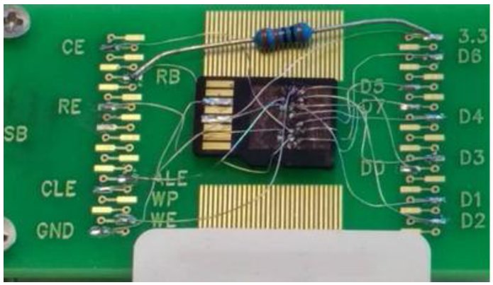
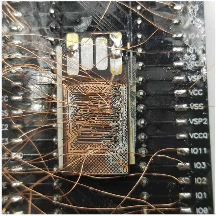
Examples of direct reading of monolithic NAND flash memory
The following images show a laboratory technique for reading the memory directly by physically removing the component and connecting its contacts to a specialist reader. They are included for information only.
This technique is reserved for devices whose controller has stopped working completely. It is not used when the controller can be brought back into operation with service microcode, because it involves irreversibly removing the memory component.
What NAND flash memory is
NAND flash memory stores information as electrical charge trapped inside each cell, and keeps it even when the device is disconnected. That is why it is the basis of SSDs, USB sticks, SD and microSD cards, and the internal storage of phones and cameras.
What distinguishes the different types of NAND is how many bits each cell stores. To store more bits, the cell has to tell apart more charge levels within the same voltage range: 2 levels for 1 bit, 4 for 2 bits, 8 for 3 bits and 16 for 4 bits. The more levels there are, the narrower the margin between them, and the easier it is for wear or a small electrical disturbance to make the cell read wrongly.

That is the underlying reason for the trade-off between capacity, cost and endurance. Endurance is measured in program/erase (P/E) cycles: how many times a cell can be written and erased before it starts to fail.
SLC: one bit per cell
With only two levels, the margin between them is wide: it is the fastest and most durable type, in the order of 100,000 P/E cycles, but also the most expensive per gigabyte. It is reserved for industrial and enterprise uses where endurance matters more than capacity.
MLC: two bits per cell
Four levels per cell double the capacity of SLC at a lower cost, with endurance in the order of 10,000 P/E cycles. For years it was the usual balance in professional equipment.
TLC: three bits per cell
Eight levels per cell lower the cost and raise the capacity, in exchange for less endurance, in the order of 3,000 P/E cycles, and a controller that has to correct more errors. It is the most common type in today's consumer equipment.
QLC: four bits per cell
With sixteen levels in the same range, QLC offers the highest capacity at the lowest cost, but the lowest endurance, in the order of 1,000 P/E cycles, and the narrowest margin. It suits high-volume storage that is written rarely and read often, such as media files or archive copies.
3D NAND: cells stacked vertically
For years capacity grew by shrinking the cells, placed side by side on the chip (2D NAND). At very small sizes the cells became less reliable. The answer was to stack them in vertical layers: 3D NAND allows more capacity without shrinking each cell further, and it can be combined with any of the types above (SLC, MLC, TLC or QLC).
Comparison of NAND flash technologies
| Technology | Bits per cell | P/E cycles (endurance) | Relative cost | Speed | Typical use |
|---|---|---|---|---|---|
| SLC (Single-Level Cell) | 1 bit | ~100,000 | Very high | Very high | Servers, industrial, enterprise |
| MLC (Multi-Level Cell) | 2 bits | ~10,000 | Medium-high | High | Prosumer, enterprise, workstations |
| TLC (Triple-Level Cell) | 3 bits | ~3,000 | Low | Medium | General consumer, laptops, PCs |
| QLC (Quad-Level Cell) | 4 bits | ~1,000 | Very low | Medium-low | Mass storage, archive |
Important notes
- P/E cycles: the number of program and erase cycles a cell can withstand before it degrades.
- Endurance: the more P/E cycles, the longer the device lasts.
- Density: the more bits per cell, the higher the storage capacity, but the lower the endurance.
- 3D technology: it can be applied to any of these technologies (SLC, MLC, TLC, QLC) to increase capacity by stacking cells vertically. The P/E cycle figures in the table correspond to the current 3D generation of each technology, so the improvement of the three-dimensional architecture over 2D is already built into those values.
- Cost-performance: SLC offers the highest performance at the highest cost, while QLC offers the highest capacity at the lowest cost.
- Read disturb: endurance expressed in P/E cycles only measures wear from writing and erasing. It does not reflect degradation from accumulated reads, which is a separate mechanism and hits higher-density technologies harder.
Additional information
Endurance compared
- SLC lasts roughly 100 times longer than QLC.
- MLC lasts roughly 10 times longer than QLC.
- TLC lasts roughly 3 times longer than QLC.
Density compared
- QLC stores 4 times more data per cell than SLC.
- TLC stores 3 times more data per cell than SLC.
- MLC stores 2 times more data per cell than SLC.
Recommended uses
- SLC: critical applications where endurance and speed are essential (servers, databases, industrial applications).
- MLC: professional use with moderate to heavy workloads (workstations, video editing, software development).
- TLC: general consumer use with light to moderate workloads (laptops, personal computers).
- QLC: high-capacity storage with moderate reading and little writing (media files, backups, archives).
Market trends
- 2000-2010: SLC and MLC dominate.
- 2010-2015: mass transition to TLC.
- 2015-2020: QLC is introduced and adopted.
- 2020 onwards: 3D NAND with TLC and QLC dominates the market.
Outlook:
- PLC (Penta-Level Cell): five bits per cell, in development.
- Continuous improvements in 3D NAND: more layers and better endurance.
- More sophisticated management algorithms to make up for lower endurance.
- Greater emphasis on energy efficiency.
Sources and references
- Kingston Technology, "Diferencias entre SLC, MLC, TLC y 3D NAND". https://www.kingston.com/es/blog/pc-performance/difference-between-slc-mlc-tlc-3d-nand
- Y. Cai, Y. Luo, S. Ghose, O. Mutlu, "Read Disturb Errors in MLC NAND Flash Memory: Characterization, Mitigation, and Recovery", 45th Annual IEEE/IFIP International Conference on Dependable Systems and Networks (DSN), 2015.
- Y. Cai, S. Ghose, E. F. Haratsch, Y. Luo, O. Mutlu, "Errors in Flash-Memory-Based Solid-State Drives: Analysis, Mitigation, and Recovery", Carnegie Mellon University, 2017 (arXiv).
- Y. Cai, E. F. Haratsch, O. Mutlu, K. Mai, "Threshold Voltage Distribution in MLC NAND Flash Memory: Characterization, Analysis and Modeling", Design, Automation and Test in Europe (DATE), 2013.
Technical analysis and writing: SOS Data Recovery Laboratory (Tecnología y Negocios del Caribe C.A.). Laboratory technical paper, version 2 revised, September 2026.
Services related to this article


